
Adaps Photonics releases ADS6311 for high resolution solid-state LiDAR
Inside solid-state LiDAR, ADS6311 is compatible for automotive, robotics and industrial applications
As a leading edge company in SPAD dToF industry, Adaps Photonics breaks through in technology and sets its foot on remarkable milestones in 2023, passing AEC-Q102 Grade 1 automotive reliability certification, achieving mass production of SiPM used in LiDARs and popular vehicles, taking honors as a specialized and sophisticated enterprise with new technology and unique products.
Now, Adaps is releasing an encouraging technology of 3D-stacking SPADIS(SPAD Image Sensor) chip with high resolution and best ranging performance in solid-state LiDAR, the ADS6311.
ADS6311 is a 3D-stacking chip consisted of an upper layer SPAD array and a lower layer logic circuit, which represents the trending technology of 3D camera. ADS6311 could be widely used in inclusive industries such as automotive LiDAR, robotics 3D slam and sensing, and industrial 3D cameras. Adaps provides ADS6311 chip and its EVK module with an optical system.
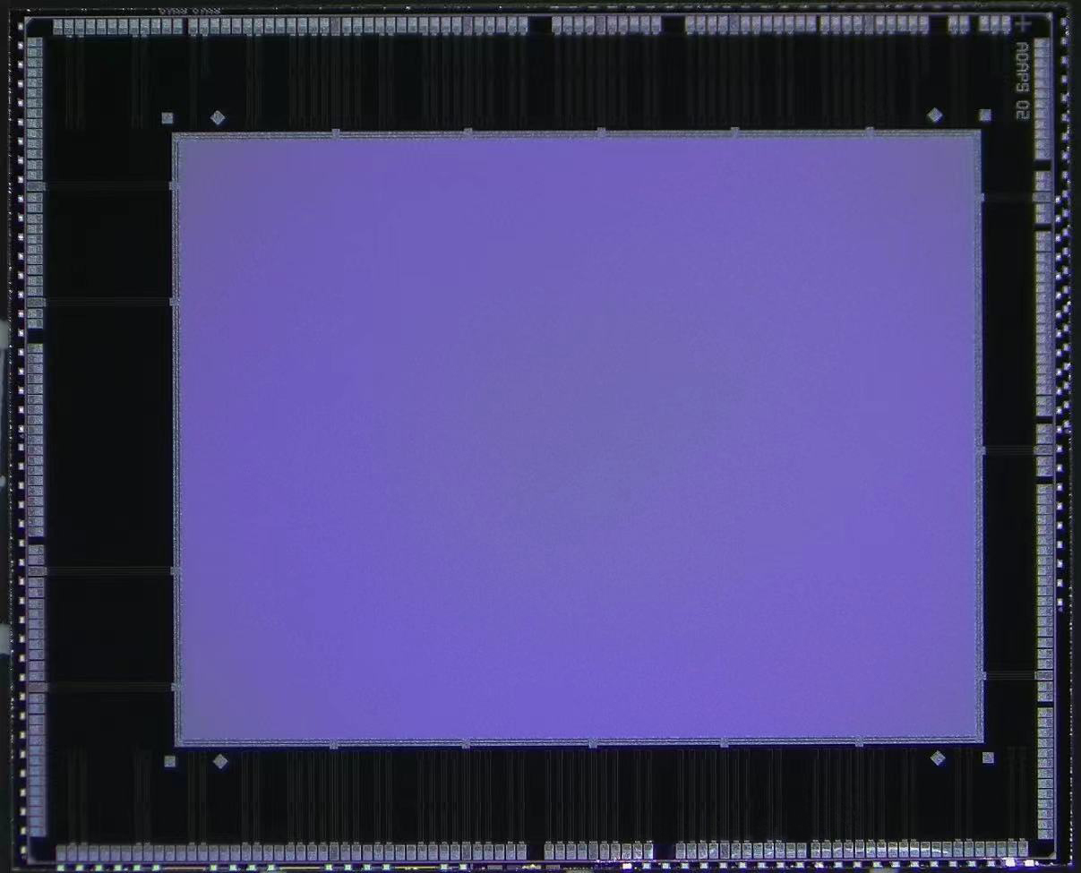

ADS6311 Chip and evaluation board
ADS6311 development and performance
The development process of ADS6311 is fast and efficient since Adaps has accumulated profound technology knowhow and development experience in 3D-stacking array chip. The tape out was finished in the early 2023 and fab out was in July. With months of synchronous development, Adaps builds software system and hardware reference design, from demo to several versions of EVK.
ADS6311 has passed multiple functionality and reliability tests. Since it is using the same processing platform as SiPM, it can also pass the reliability test and achieve mass production, regarding Adaps SiPM has been qualified for AEC-Q102 Grade1 level, and the only difference in the upper layer is its pixel connection patterns between parallel connection in SiPM and array arrangement in SPAD.
From 2018 when Adaps Photonics was founded, the dev team has endeavored every effort to iterate the SPAD array from a small size to a large scale, back to the initial ones with 80x60 and 160x120 resolution, and the former generation ADS6303 of 240x160 resolution(mass produced in 07/2021). This new born generation of ADS6311 has reached an unprecedented level, 768x576 pixels! Four times to IMX459 and forty-three times to ibeonext.
Worldwide, only a few companies are capable of such high-end technology in automotive industry. Adaps is making consistent technology innovation in SPAD resolution, ambient light resistance and ranging performance. By combining 3x3 pixels to a mega pixel, ADS6311 has realized 256x192 cloud points and around 1M points per second in the cloudpoints map.
During the development procedure, ADS6311 generated the cloudpoint map in the very first smoking test successfully and showed a stable and precise cloudpoints output. Solid-state LiDAR requires high performance SPADIS chip on its spec in every perspective, in order to ensure the performance of the LiDAR on a system level. Adaps holds strong technical barriers in this territory, including prominent SPAD layer, highly integrated analog and digital stacking design, specialized LiDAR DSP and automotive level reliability and packaging.
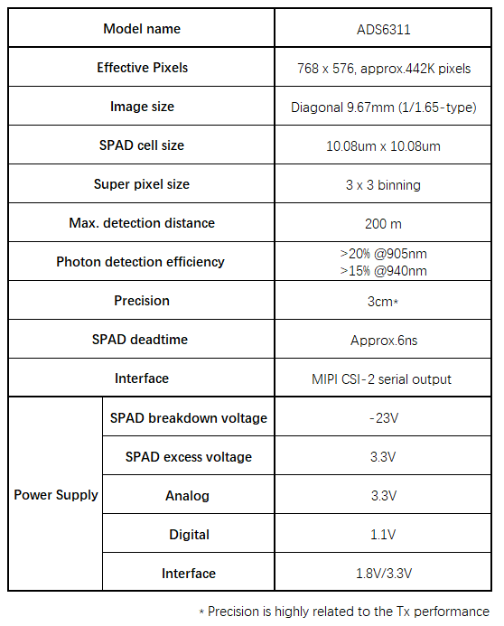
ADS6311 spec datasheet
The advantages of ADS6311 are: (a) superb resolution to guarantee the 3D imaging quality; (b) generations of 3D-stacking iteration and verification in mass production; (c) AEC-Q automotive level performance and reliability; (d) advanced DSP on chip algorithm for accurate and high frame rate cloud points; (e) easy to use with low requirement on SOC or FPGA; (f) compatible for both 1D and 2D scanning; (g) compatible for ADAS LiDAR and blind coverage corner LiDAR.
Based on ADS6311, Adaps has developed large FOV 120*90° LiDAR EVK, also with a small FOV optical and system design, ADS6311 could be used as ADAS LiDAR in a way of multiple chips combination or a single chip with scanning system. Through such a universal design, we achieve the solid-state SPAD array's utility in its application industries and working conditions.
ADS6311 applications and market outlook
It is commonly recoginised by the industry that LiDAR technology walks from hybrid to solid-state, by using SPADIS and VCSEL arrays. ADS6311 is the second generation of Adaps's large scale array product, facing the EV and AMR robotics smart sensing markets.
In recent years, NOA draws huge attention in intelligent vehicles. ADS6311 is suitable for L2~L4 EV in low speed cases like auto parking, AEB, auto following in a traffic jam and collision alert and avoidance in turning. Through realizing 3D environment reconstruction, such LiDARs solve high frequency problems for customers in their daily life in a most intuitive, visible, and sensible way.
We can see effects from the tests below, the cloudpoints map is 256x192 mega pixels and the grayscale image is from 768x576 SPAD pixels, which equals to 440K pixels. The coaxial imaging data makes ADS6311 getting both image and its depth data at the same time and in exactly the same frame. Adaps is optimizing the pixel pitches to a smaller size and superior performance. Larger cloudpoints and grayscale image makes popular CV algorithm migrate consistently from 2D CIS to 3D SPADIS. With pixel pitch becoming smaller and smaller, the scale effect will show up in SPAD image sensor as it happened in the CMOS CIS industry on Silicon.
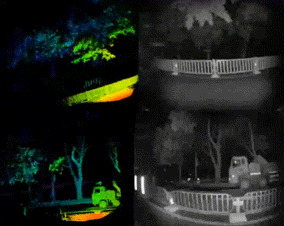
Roadside(change the visual angle to feel 3D) and opposite lane
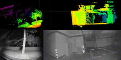
Non-motorized vehicle lane and parking lot
Meanwhile, LiDAR BEV transformer provides a surrounding model and 3D view, trying to reconstruct city streets and blocks with splendid moving vehicles could be realized in the first time for humanity. 3D depth model and 2D pictures are captured at the same time in a same frame just like the combination of bones and skins.
In the V2X end, ADS6311 supports high frequency and accuracy surveillance on the lanes and crossroads, making the municipal transportation upgrade to a digital system become possible. Emerging market roots on such city level digital twins is foreseeable in a near future.
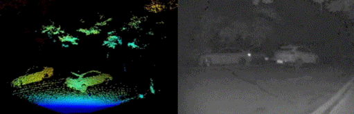
Vehicle lanes surveillance
Crossroads surveillance
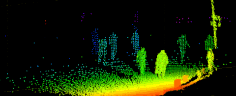
As a standardized SPAD array chip, ADS6311 is valuable in the robotics market, industrial market and some long-tail markets. Realtime and high frequency depth capture ensure it works as a stable and accurate depth data source in circumstances like complex scenarios, multipath interference cases, long short detection switching, glass detection, ambient light resistance, etc.

High frequency capture (GIF resolution compressed) and 3D modelling

768x576 Grayscale of blood vessel
ADS6311 is the choice for the following industries, feel free to contact us through email: sales@adaps-ph.com
● Passenger vehicles, commercial vehicles, industrial vehicles
● Service, working, humanoid robots
● AGV, AMR, small carriers
● Smart household, smarting building, V2X lanes and industry surveillance
● 3D scanning, posture control, motion capture, 3D imaging
● 3D data gathering, algorithms training, scientific research and lab collaboration
ADAPS PHOTONICS
Single Photon Avalanche Diodes (SPADs) are core components of 3D perception in modern electronic devices, enabling smarter cars, phones, robots, autonomous control, and human-machine interaction. Established in 2018 to commercialize leading edge SPAD research, Adaps Photonics creates eyes for a smart future by providing SPAD-based dToF sensor chips and system solutions. Our products deliver industry-leading accuracy, distance, and power efficiency.
Adaps Photonics provides a family of SPAD-based sensor products: SiPM, 3D-stacked dToF module, and all-in-one dToF depth sensor. Our most advanced 3D-stacked module consists of a BSI sensor array die hybrid-bonded to a custom DSP die to achieve the highest performance and density in the industry.
Top-tier companies in the automotive and consumer electronics industries have chosen Adaps Photonics for our competence to deliver superior products in volume by sourcing from multiple foundries and a robust global supply chain. Our development process complies with ISO 9001. Our automotive products, produced by a supply chain qualified for IATF16949, are set to be certified as qualified for AEC-Q100 and AEC-Q102.
Copyright © Adaps Photonics All rights reserved  粤公网安备号44030502004595 粤ICP备19128428号-1